With a market expected to reach $74 billion in 2030, printed electronics provide flexible, lightweight, and new form factors for electronics in diverse applications. With the aim to minimize material waste and production costs, by eliminating parasitic support structures and reducing the amount of wiring and complexity in the structure, printed electronics are increasingly recognized as a key enabler for the Internet of Things as part of the “Fourth Industrial Revolution”.
Stretchable materials can be used to create functional electronics like RFIDs, solar cells, LEDs, and transistors. The combination of stretchable sensors, actuators, and displays can be used to create real, tangible displays and friendly HMIs on all kinds of surfaces, especially 3D.
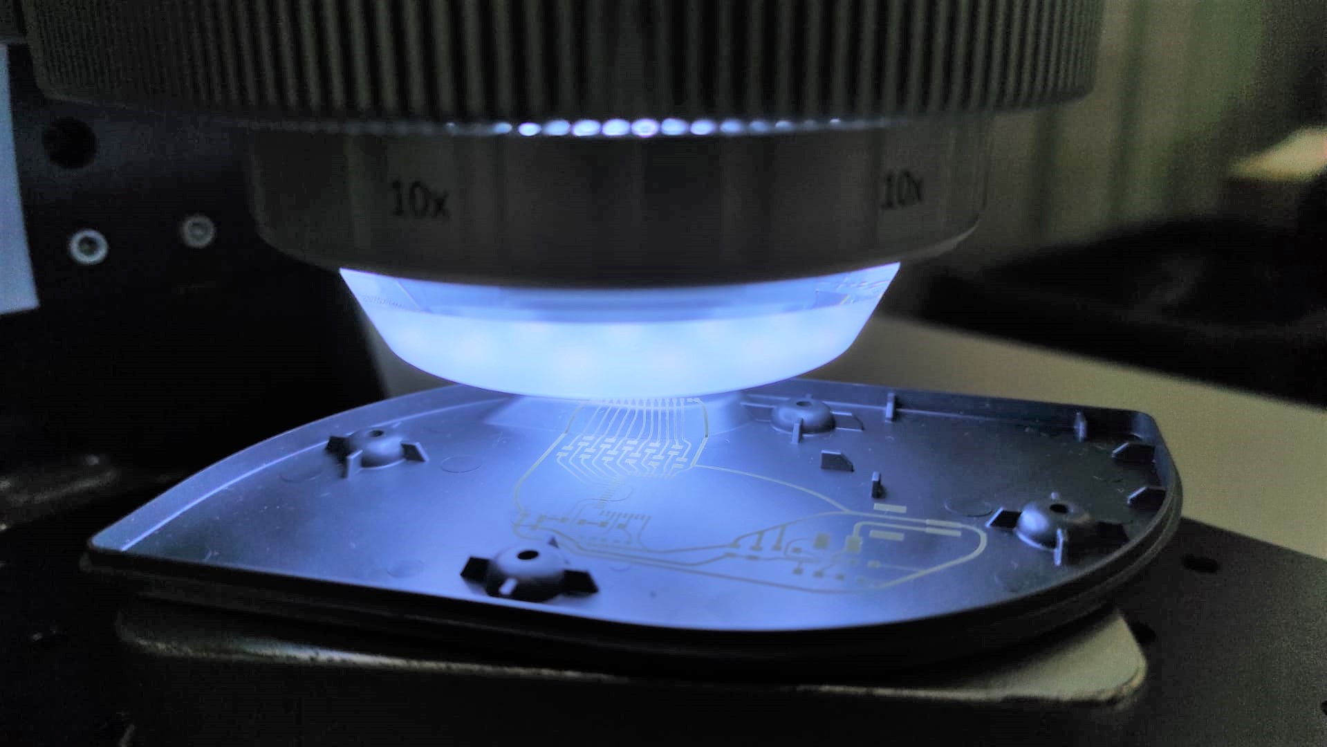
A good-established approach to incorporate electrical functions onto the surface of 3D objects is Laser Direct Structuring (LDS), in which an additive in the injection moulded plastic is selectively activated by a laser. This process forms a pattern that is subsequently metallised using electroless plating. LDS saw tremendous growth around a decade ago and is used to manufacture hundreds of millions of devices each year, of which around 75% are antennas.
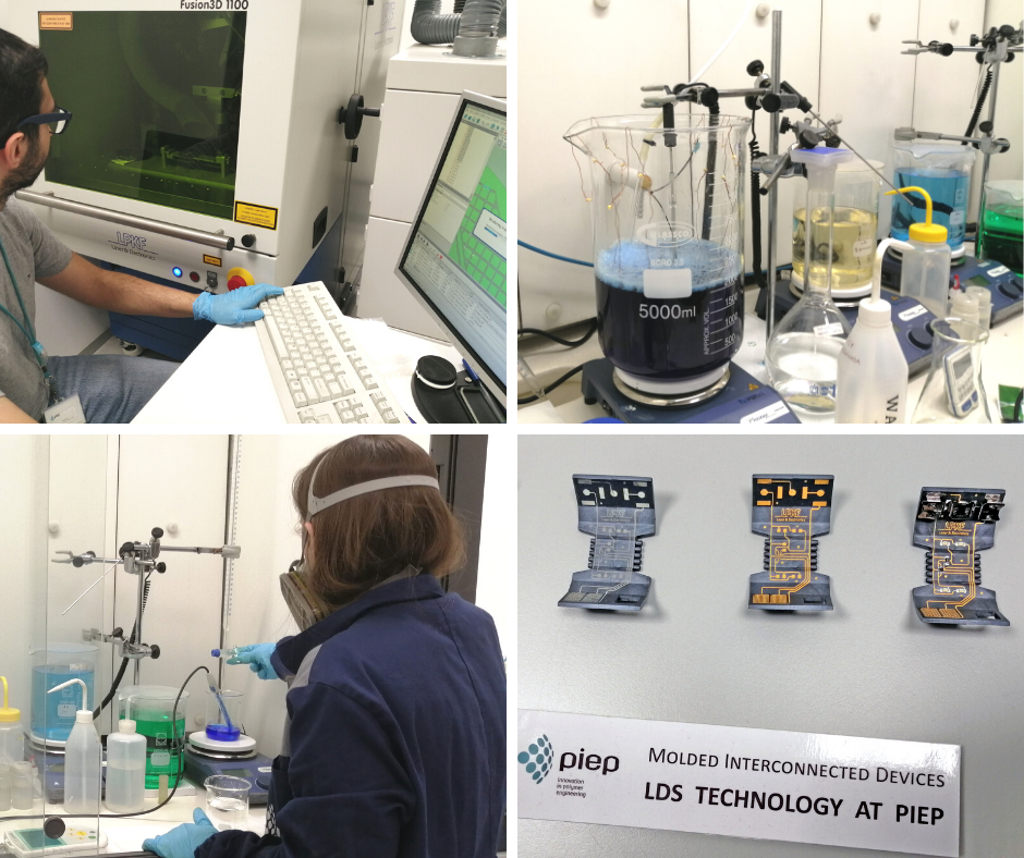
Laser Direct Structuring (with LPKF Fusion 3d 1100 and chemical baths) at PIEP
However, LDS has some weaknesses. A low resolution compared to other processes and a single layer of metallisation leave space for alternative approaches. One of these is called In Mould Electronics (IME). The basic principle is applying conductive traces directly onto a thermoformable substrate, and SMD components mounted using conductive adhesives. The substrate is then thermoformed to the desired shape, and infilled with injection moulded plastic. IME is especially well suited to HMIs in both automotive interiors and the control panels of white goods since decorative films can be used on the outer surface above capacitive touch sensors.
Regarding the materials used in these processes, they play a critical role as in almost any new electronics program. Polymers used in LDS and flexible electronics include PET, LCP, and PC, among others. For efficient performance of the electronic devices, concerns regarding humidity, thermal and dimensional stability, and solvent resistance need to be taken into account.
Despite some technical and process attractions and virtues of LDS, sensors, and electronics are key enablers for the future of the industry and its applications. This way, by reducing manufacturing complexity, lowering weight, and enabling new form factors – since rigid PCBs are becoming no longer required – hybrid electronics can bring the best of both worlds to a wide variety of non-traditional and innovative devices and technologies.
Acknowledgments
Work developed in the scope of iDOURECA project (n.45113), which was co-financed by Portugal 2020, under the Operational Program for Competitiveness and Internationalization (COMPETE 2020) through the European Regional Development Fund (ERDF).

Authors:


Ricardo Freitas, Luciano Rietter, Bruno Vale – PIEP – Pólo de Inovação em Engenharia de Polímeros
Maria João Lopes – CeNTI – Centre of Nanotechnology and Smart Materials
Sónia Gomes – Doureca Produtos Plásticos Lda

